


Labs
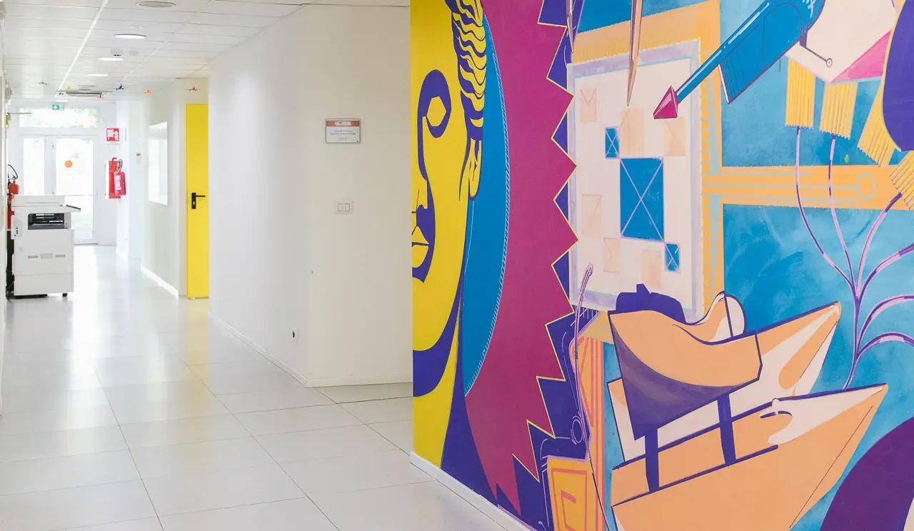
Where we make innovation
What would scientific and technological know-how be without the right equipment? One of our assets is to work within facilities equipped with state-of-the-art technology. This, combined with our own and our strategic partners’ human capital, allows us to constantly innovate.
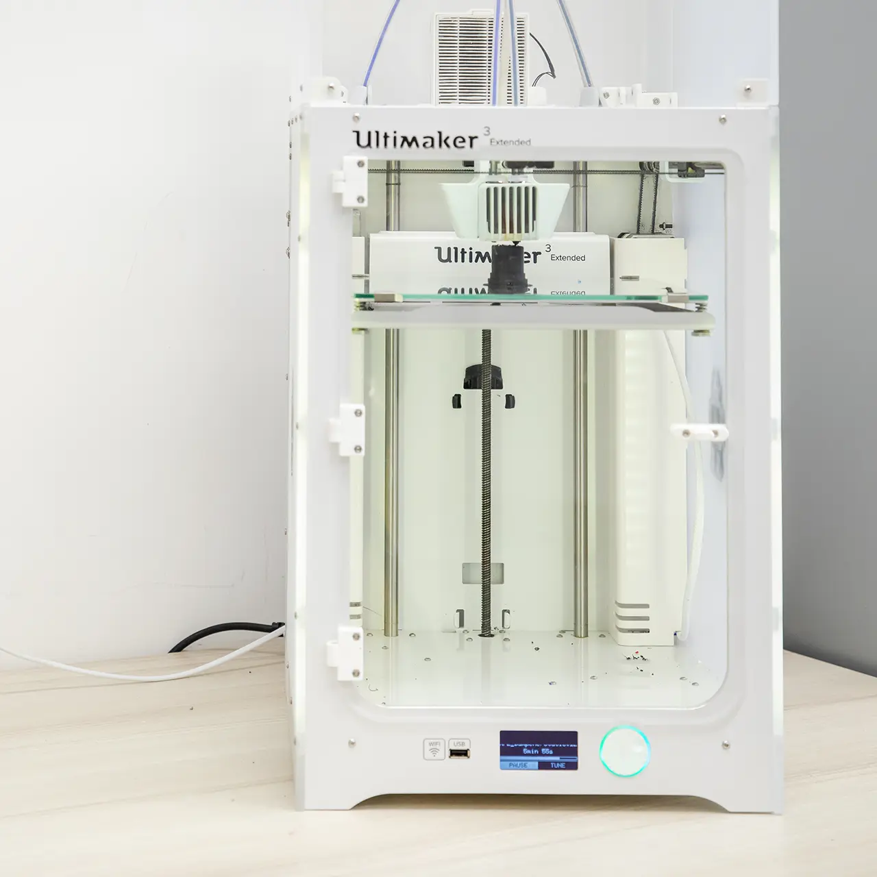
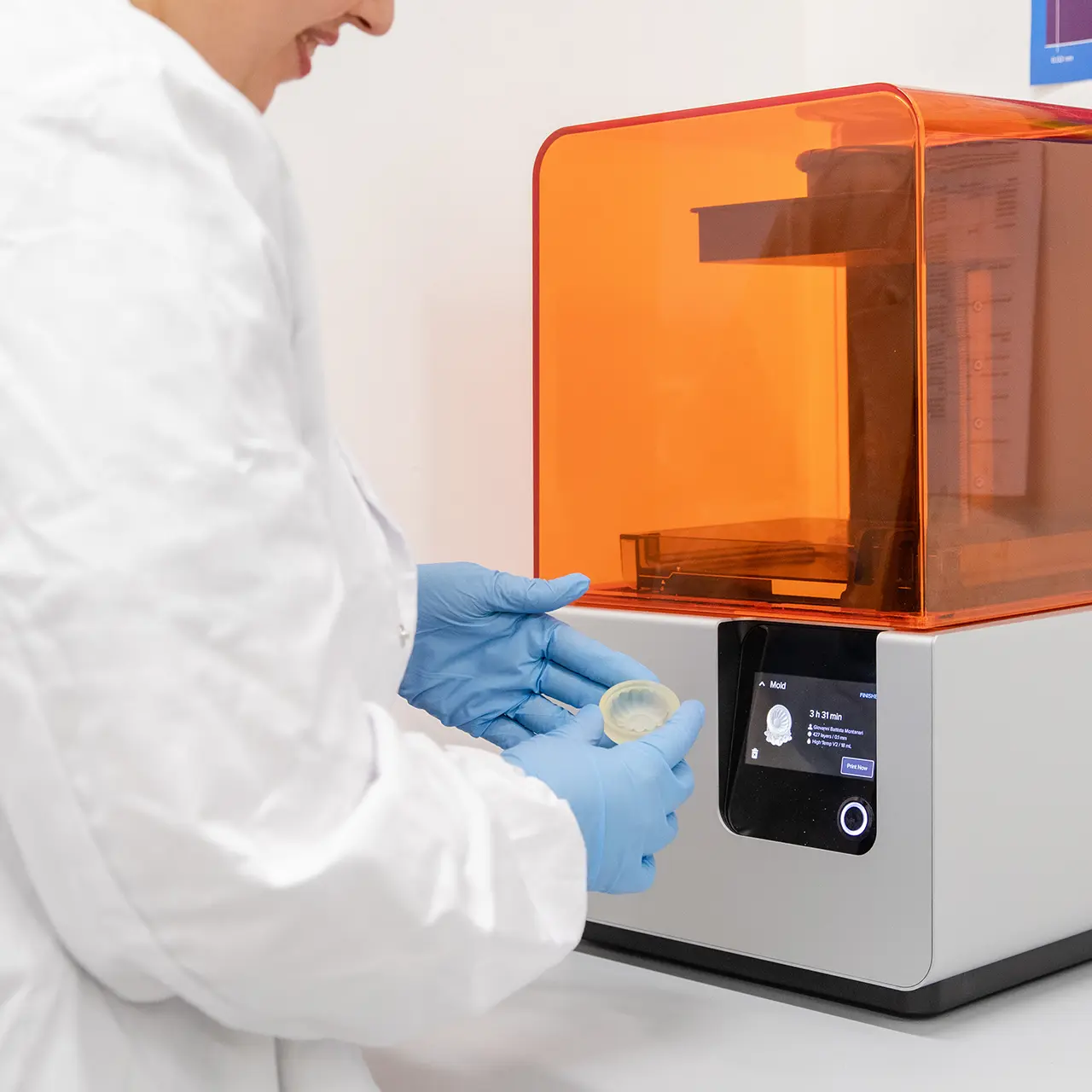
Prototyping Lab
In this lab we deal with CAD design and fabrication of mechanical parts using one FDM and one SLA 3D printer.
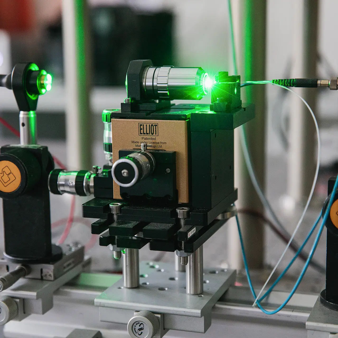
Optics Lab
We use the optical table for setting up optical and spectrometric characterization of devices.
It is also possible to characterize various liquid and thin-film substances in different spectral windows ranging from UV to MIR.
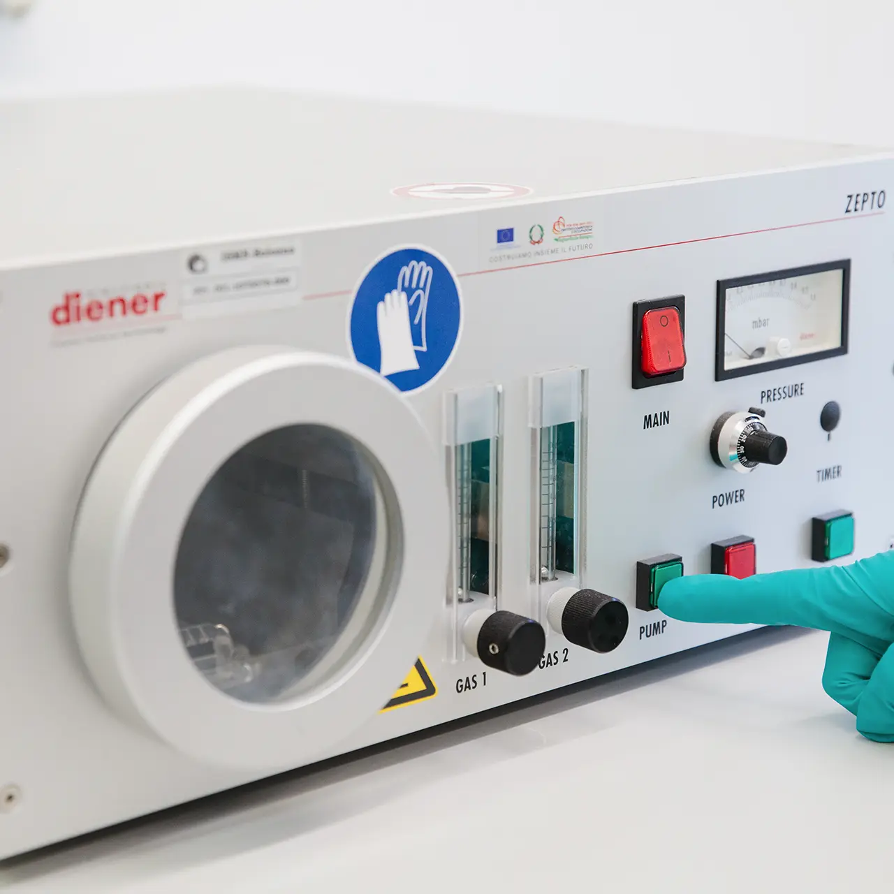
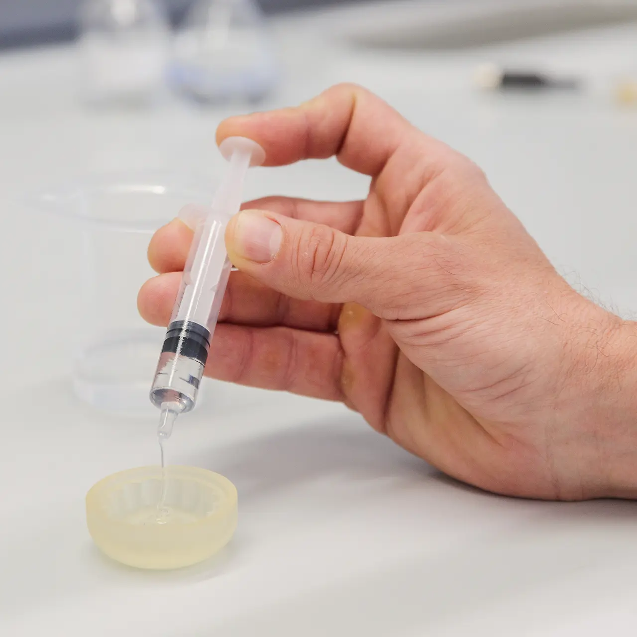
Chemistry Lab
Here we design and develop innovative materials and manufacture transparent silicone devices obtained using resin molds.
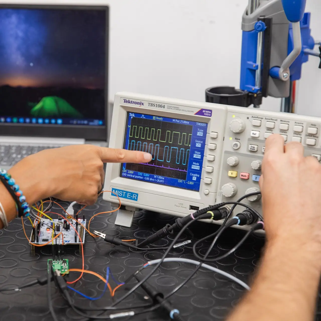
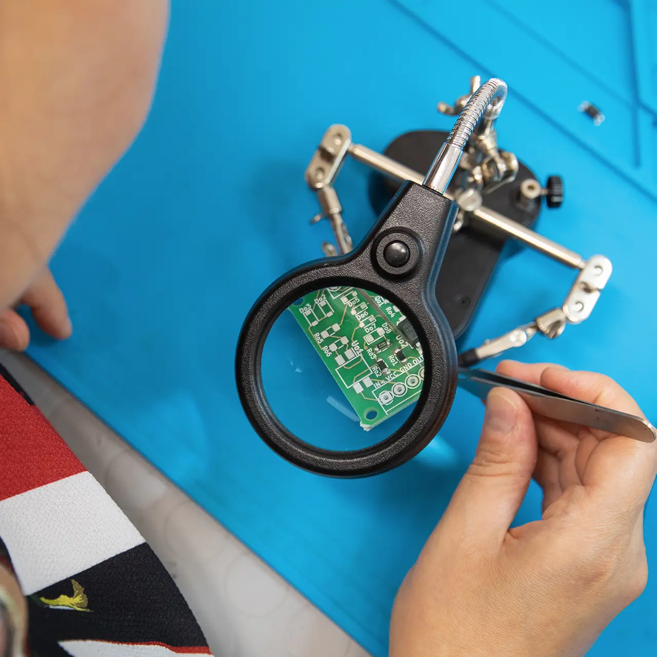
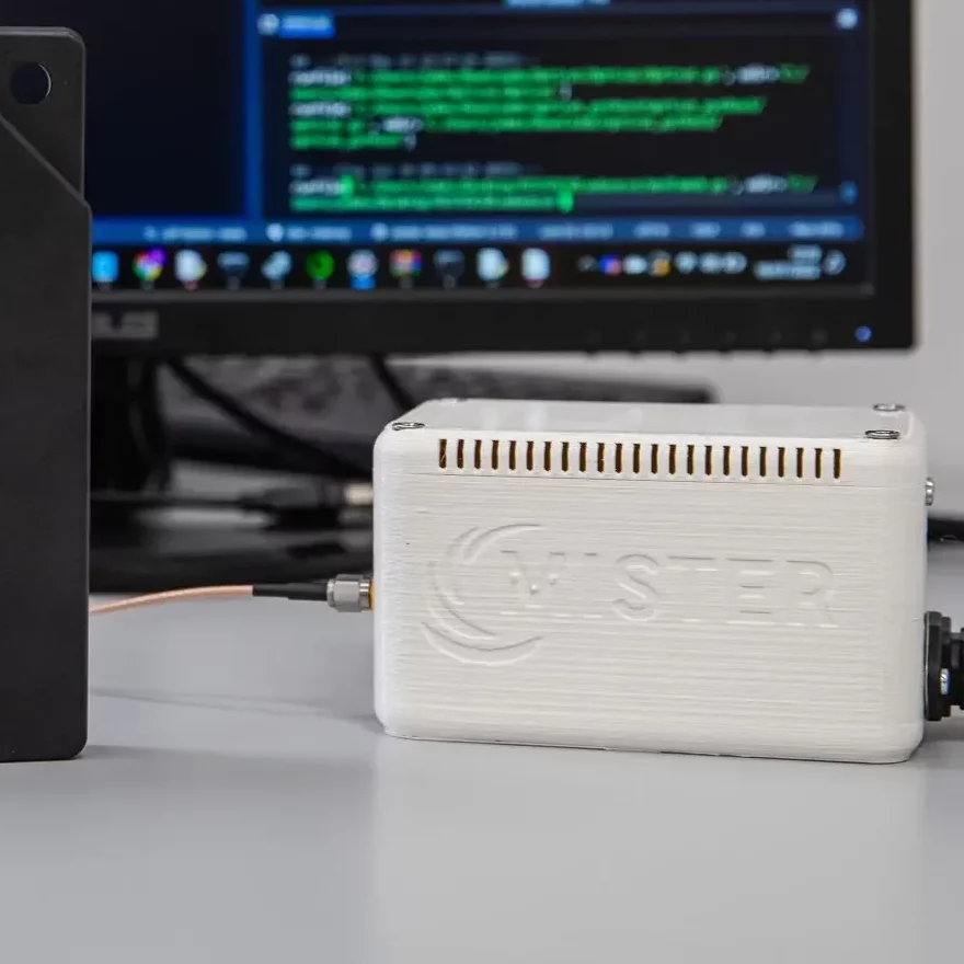
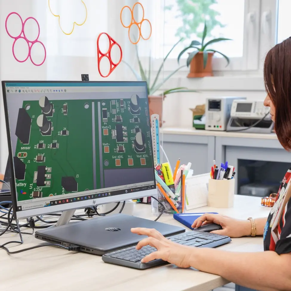
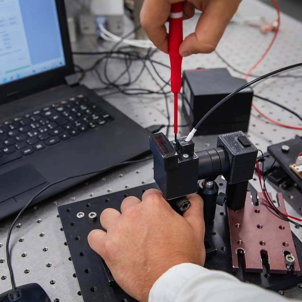
Electronics Lab
In this laboratory, boards with sensors and microcontrollers are designed, tested and assembled and their packaging is created using additive and/or subtractive manufacturing.
Certified measurement instruments are also available for testing the devices.
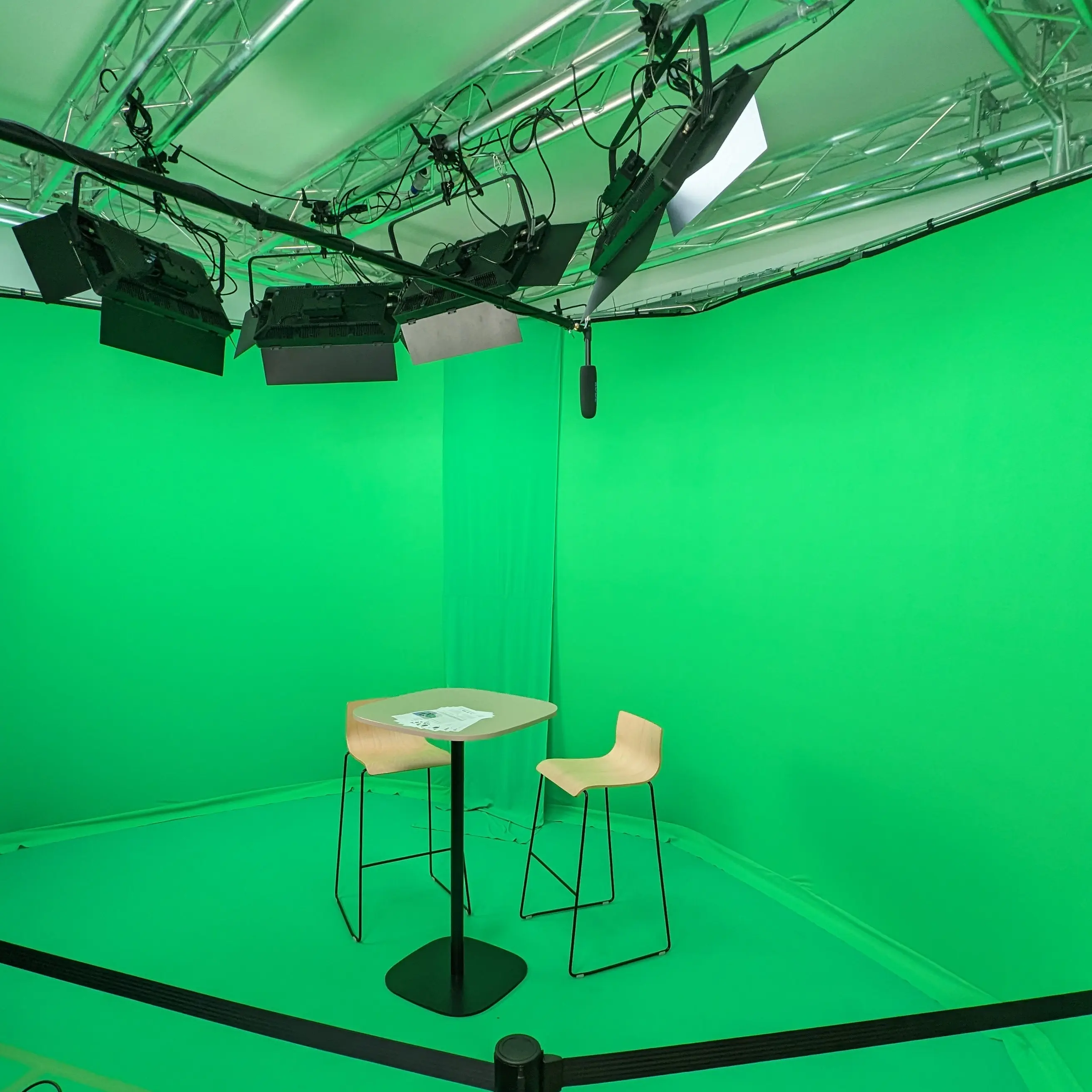
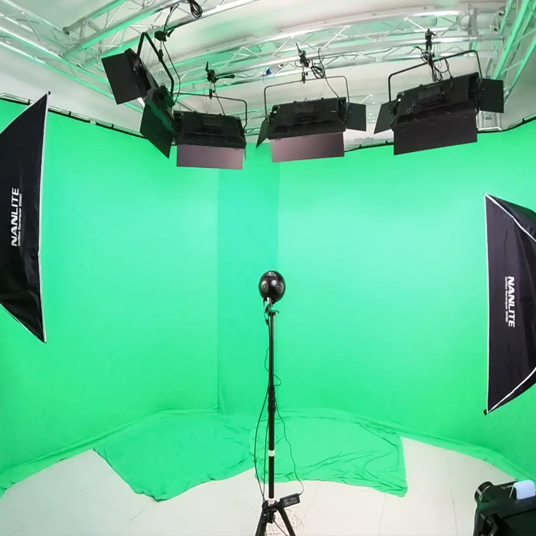
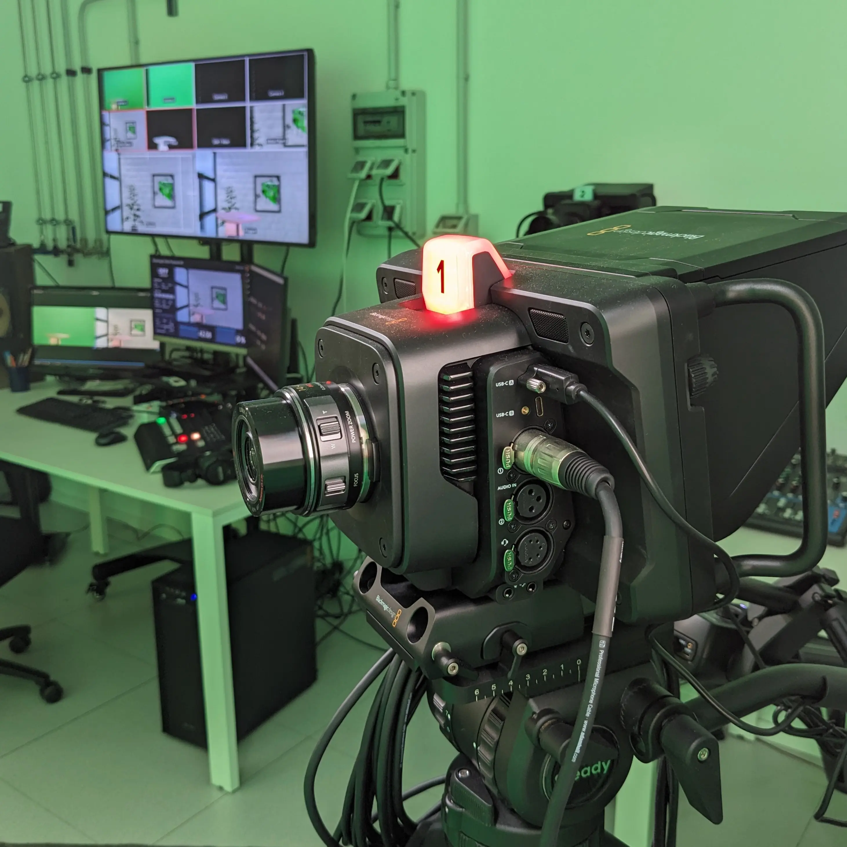
Virtual Studio
Our Virtual Studio is in line with the latest broadcast standards and includes: a panoramic green screen (180°+), 4k director and cameras, ambisonic microphone, led lighting on beams, lighting control system and workstation to handle video streams up to 8k.
Thanks to the strong bond with Bologna CNR research institutes, MISTER staff has access to some additional labs and equipment.
Manufacture
The IMM institute has the largest public facility in Italy for micro and nano fabrication of devices made of silicon and other materials. The clean room covers an area of 500 m2 and is divided into three zones with different cleanliness levels.
All the main technologies required for the fabrication of MEMS (Micro-Electro- Mechanical-System), NEMS (Nano-Electro-Mechanical-System) and MOEMS (Micro-Optical- Electro-Mechanical-System) are available in the clean room.
Located at the ISMN and ISOF, they are the place where research on development of functional and biomimetic materials and the fabrication of biodiagnostics devices are carried out. They are equipped with instruments for the evaluation of molecular and functional aspects both high throughput and on single in-vitro cells.
The expertise present within the laboratory allows to: manipulate primary cell preparations and secondary cell lines, perform cell vitality and biocompatibility assays, perform molecular and gene expression studies (PT, PCR, Elisa, WB), perform functional studies of membrane proteins (Calcium Imaging, Patch Clamp and extracellular recording through MEA).
Located at the ISOF this lab is equipped to carry out organic synthesis procedures of molecular, macromolecular and hybrid organic-based systems. The laboratory is equipped with instrumentation suitable for both conventional (ambient atmosphere, controlled atmosphere and vacuum) and non-conventional (microwave-assisted synthesis) organic synthesis.
Located at ISOF and is used for the synthesis and functionalization of new two-dimensional materials such as graphene and boron nitride. The synthesis techniques used (sonication – milling – homogenization) are easily scalable from an industrial point of view. In addition to synthesis, the laboratory is also equipped with specific equipment for the characterization of the manufactured materials. The analytical techniques used are: probe microscopy, laser particle size, surface area and electrical measurement. In addition, polymer composites can be made in the laboratory with graphene and other 2D materials both as thin films and in bulk.
Characterization
The nuclear magnetic resonance (NMR) spectrometer enables both conformational and configurational studies of molecules of interest. Through the NMR technique it is possible to study: interactions between molecules in space, ligand-receptor interactions, measurements of relaxometric parameters and diffusion coefficients.
In addition, it is possible to quantify analytes in even very complex matrices. Such studies can be carried out on samples in solution, solids and semisolids of small organic molecules, tissues and biological samples, emulsions, foods, seeds, organic and inorganic materials (nanostructured and non-structured), polymers, and complex matrices.
Located at ISOF, this system allows quantitative and non-destructive compositional analysis of industrial samples such as coatings and thin films by X-ray photoemission electron spectroscopy (XPS).
In particular, surface mapping with a The state of surface cleanliness and orderliness can also be checked by electron diffraction (LEED) measurements.
The state of surface cleanliness and orderliness can also be checked by electron diffraction (LEED) measurements.
The instrumentation also includes an STM microscope.
Located at the ISMN, the femtosecond laser is used as an excitation source for the identification and characterization of transient species with lifetimes in the fs – ns range. The streak system allows the measurement of luminescence of materials in solution or solid-state with ultrashort ( 1 ps) time resolution.
Located at the IMM, the diffractometer can perform X-ray scattering measurements in a wide angular range and with different sample diffraction planes. The available optical elements also enable high angular resolution measurements, which are necessary for the characterization of materials of high crystallinity.
The Scanning Electron Microscope (SEM) is used in the morphological and analytical characterization of materials and in electrical measurements on sub-micrometer-sized electronic devices. The instrument is also equipped with an EDS spectrometer that enables compositional analysis at the sub-micrometer scale.
The Transmission Electron Microscope (TEM) is used to characterize the microstructure of materials at very high spatial resolution. By combining high-resolution imaging techniques with electron diffraction, it is possible to derive crystal structure information and analyse possible defects with nanometer-level spatial resolution.
Located at the IMM, it is equipped with a probe station for the parametric characterization of electronic, electromechanical and/or semiconductor devices.
The probe station has 4” thermo-chuck that can be adjusted from room temperature up to 300°C.